

SIMULATION_Hub
Simple, web based and pluggable Simulation Solution
Simulation_Hub
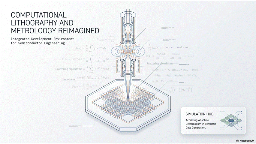
Simulation Hub 2026 is an innovative computational metrology and lithography platform that seamlessly balances rigorous mathematical precision with an intuitive, user-friendly interface. The application features highly flexible operational modes, including a CAD-to-SEM generator for synthetic data creation, a Profile-to-SEM mode for rapid physical extrusion, and a See-Through mode for complex subsurface backscatter electron modeling. By unifying rigorous physics, integrated artificial intelligence for proxy model training, and streamlined parameter management, Simulation Hub democratizes advanced semiconductor modeling and significantly reduces costly fabrication calibration time
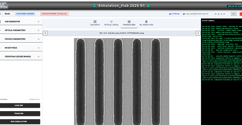

Simulation_Hub CAD2SEM mode
CAD to SEM mode seamlessly transforms 2D binary CAD layouts into highly realistic scanning electron microscope (SEM) images. It leverages a dual optical simulator that allows users to choose between the lightning-fast Hopkins SVD method or the highly rigorous Abbe integration. Users can easily generate synthetic data using an automated pattern library and inject highly realistic stochastic defects, line edge roughness, and quantum noise. Furthermore, this mode natively embeds a neural network engine that instantly captures your active physics settings to train bespoke deep learning proxy models.
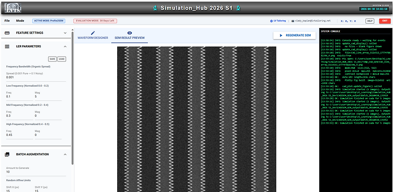
Simulation_Hub Profile2SEM mode
Profile to SEM mode redefines rapid physical extrusion by enabling users to design 1D surface topologies on an interactive 30-point waveform canvas. This flexible approach bypasses heavy optical simulation, seamlessly extruding the drawn profiles into infinite 2D trenches or wrapping them into 360-degree contacts. A built-in batch augmentation module revolutionizes machine learning dataset creation by applying randomized affine transformations on the fly to produce thousands of unique training frames. By supplying a mathematically precise and deterministic sample, this mode serves as an impeccable ground truth calibration standard to rigorously benchmark independent metrology inspection algorithms

Simulation_Hub See-Through mode
The See-Through mode simplifies complex subsurface backscatter electron (BSE) physics modeling by allowing users to dynamically build multi-layer material stacks. It provides an elegant interface equipped with an integrated material database and a live 2D stack visualizer for immediate geometric validation. Its standout feature is a multivariable optimization engine that mathematically sweeps physics equations to pinpoint the optimal primary beam energy, current, and dwell time. By intelligently maximizing the signal-to-noise ratio and preventing electron dose saturation, this mode automates calibration and saves immense amounts of costly fabrication time

Why LVTailoring?
Same Hardware
No need for new, highly-specialized, and expensive hardware
Same System
Re-invest in the power of your business with our innovative solution
New Capabilities
Control your capital costs, solve your performance issues and achieve your goals with ease
Save your capital dollars.
Allow us to unlock the full potential of your existing tools – using the same system, same hardware , and new software - for brand new capabilities.